


With this announcement, Samsung also ensures the attention of numerous companies wishing to obtain production capacity using the most advanced technology, since TSMC, no matter how much effort it is making to expand, cannot keep up with the entire industry.
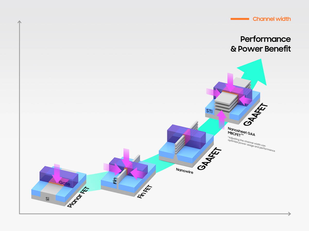
Based on a Gate-All-Around (GAA) transistor architecture, Samsung nodes are in theory a significant improvement over those made using FinFET transistors, and will serve as a springboard for the launch of progressively more refined processes.
Samsung claims that the benefits provided by its new 3nm process are remarkable, with a 45% reduction in power consumption and a 23% performance improvement over its old 5nm process. It would also allow the area to be reduced by 16%, giving rise to the creation of potentially smaller processors (although there will be firms that simply want to take advantage of that density to introduce more transistors in the same surface).
Interestingly, Samsung already dares to talk about the improvements that will come to this technology over time. According to the South Korean firm, the second generation of its node will raise energy savings to no less than 50%, while the improvement in performance will be 30% and the reduction in surface area is estimated at 35%.
Samsung has not communicated the names of the companies for which it is already manufacturing components, but firms such as Qualcomm and Nvidia may already have their production quota secured. It will be more interesting to know what happens with others like Intel and MediaTek, which could be open to diversifying their suppliers.

Add Comment