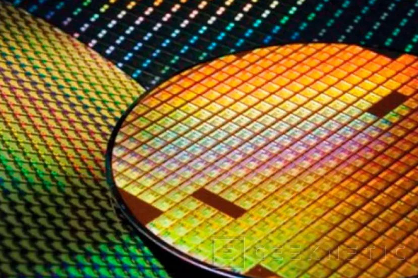
Traditionally, wafers that emerge in advanced chip manufacturing facilities have a circular shape due to how these substrates are manufactured starting from a silicon center that expands circularly towards the ends. This means that, among other things, since the chips have a generally square or rectangular design, the edges of the wafer cannot be used 100%.
New leaks They refer to the fact that TSMC, one of the leading chip manufacturing companies, responsible for the creation of processors and graphics for AMD, NVIDIA, APPLE, Qualcomm, etc. and even of the Intel Lunar Lake; is working on new packaging processes that use substrates arranged in a rectangular panel instead of traditional circular wafers.

The company would be experimenting with 510 x 515 mm size plates, which would give them the option of having a usable area 3 times larger than that of standard 12-inch wafers (approximately 314.8 mm). Not only because of its larger size, but because of its own form factor, all substrates could be used to the extremes.
Information suggests that Intel and Samsung are also testing these new formats for the future. It is clear that the first chip manufacturing company to achieve a viable process in square formats will have a significant competitive advantage.
End of Article. Tell us something in the Comments!

Antonio Delgado
Computer Engineer by training, editor and hardware analyst at Geeknetic since 2011. I love to tear apart everything that passes through my hands, especially the latest hardware that we receive here for reviews. In my free time I tinker with 3D printers, drones and other gadgets. For anything, here you have me.


Add Comment