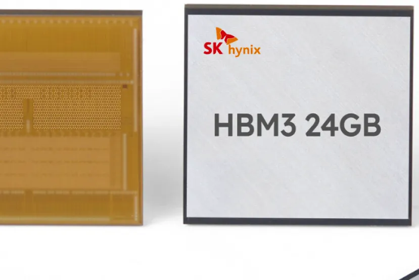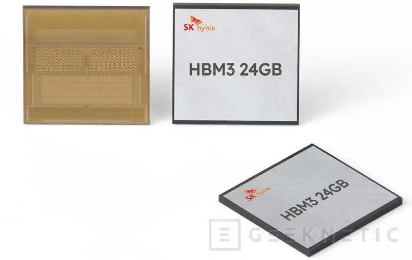
SK Hynix has announced which already has the first third-generation high-bandwidth memory chips (HBM) with 12 layers ready for shipment to customers and collaborators, that is, 12-layer stacked HBM3 memories.
Thanks to the vertical stacking of 12 layers in each chip, it is achieved that each one reaches 24 GB capacity, It can be used in high-performance systems that require large amounts of memory. For example, a GPU with four of these chips would have 64 GB of capacity.

This is a 50% increase in capacity from its previous generation of memory of this type, keeping the same size and allowing capacity to be expanded without requiring more space on the PCBs. In terms of height, they measure the same as the 16 GB modules thanks to the use of TSV (“Through Silicon Via”) technology that allows the different layers to be interconnected with an electrode that connects them vertically through thousands of small holes.
This technology has previously been used in conventional DRAM chips, and has been used by SLK Hynix in their 12-layer HBM3s.
At the moment, these chips are already being shipped to interested customers at the same time that performance tests are carried out before they are released on a large scale.
End of Article. Tell us something in the Comments!

Anthony Delgado
Computer Engineer by training, writer and hardware analyst at Geeknetic since 2011. I love gutting everything that comes my way, especially the latest hardware that we receive here for reviews. In my free time I mess around with 3d printers, drones and other gadgets. For anything here you have me.


