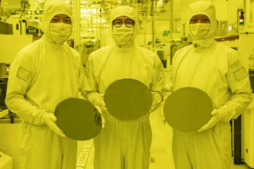
At the end of last year, several reports referred to Samsung’s alleged problems in achieving a viable yield above 70% in its 3-nanometer manufacturing process. Yield refers to the performance of the process and is measured in the % of viable chips obtained per wafer.
Now, the Korean company has come to the fore to ensure that Its 3-nanometer process has stable performance and yield and there are no problems in that regard.claiming that the company’s plans for the second generation of its 3-nanometer process with GAA (Gate All Around) technology, which replaces the previous FinFET, are being met.

The first chips to be manufactured using the second generation of Samsung’s 3nm process are expected to be the company’s own processors, starting with the Exynos W1000. This SoC is aimed at smartwatches like the upcoming Galaxy Watch 7 and would be one of the most benefited by the efficiency gains that the jump to 3nm should bring.
With low consumption, it would be able to improve the performance of the current generation by up to 3 times.
End of Article. Tell us something in the Comments!

Antonio Delgado
Computer Engineer by training, editor and hardware analyst at Geeknetic since 2011. I love to dissect everything that passes through my hands, especially the latest hardware that we receive here to do reviews. In my free time I tinker with 3D printers, drones and other gadgets. For anything you need, here I am.


Add Comment