The Challenges of Moore’s Law
Moore’s Law is a postulate made by one of the founders of Intel, Gordon E. Moore, which indicates that the number of transistors that can be integrated into a processor doubles every two years. Over the years these postulates have been fulfilled, however, as we approach smaller manufacturing processes, the physical limits of silicon are making it more difficult to maintain this progression with traditional technologies and its evolution has been slowing down.
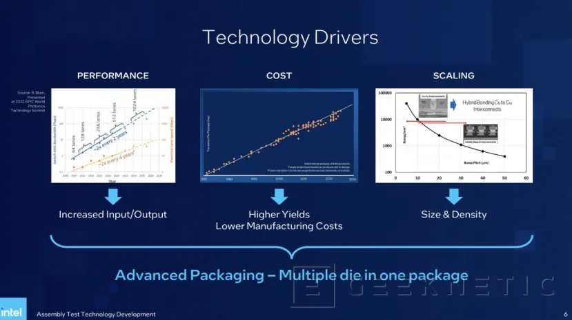
The latest trends in the semiconductor market have opted for manufacturing technologies based on chiplets that combine different Dies with differentiated functions and integrated into a single chip, combining different types of manufacturing processes that are combined on a substrate that communicates these different “tiles” to form a complete processor made up of several parts.
Combining several of these Dies or chiplets allows reducing costs by separately manufacturing smaller modules with which higher yields (number of functional chips per wafer) are achieved, while at the same time greater scalability in density and size can be achieved as they are integrated. more or fewer components on a single processor.
This allows us to continue increasing the density of processors generation after generation to try to comply with Moore’s Law.
Intel’s current Advanced Packaging Technologies
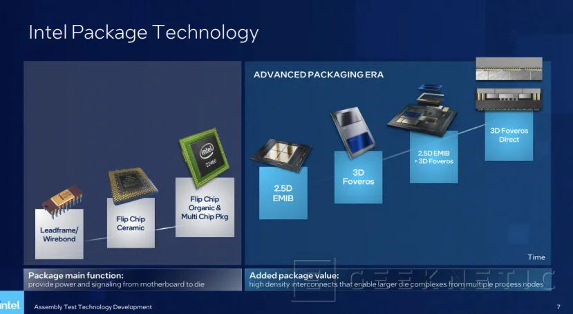
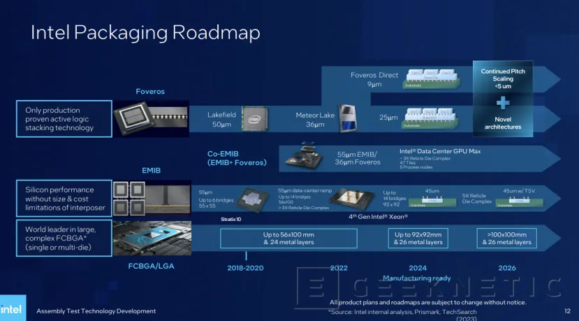
Intel has entered into what they call the “Age of Advanced Packaging”, where chiplets have taken the lead and have been combined with high-density interconnection systems that allow Dies of different sizes and manufacturing processes to be joined together. From 2.5D EMIB technology to Foveros, technologies that have been used in hybrid processors such as Raptor Lake and combined in 2.5D EMIB + 3D Foveros, until reaching the most advanced technology called 3D Foveros Direct.
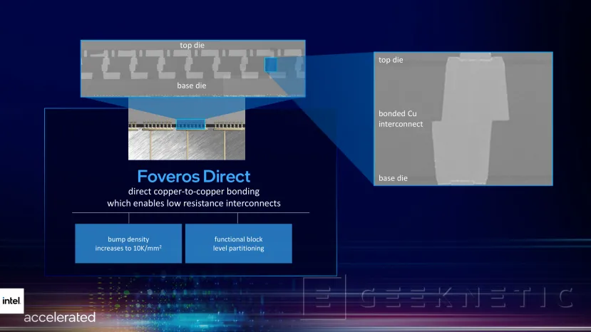
3D Foveros Direct introduces a direct copper interconnection system that reduces the resistance of the vertical connections between the different stacked dies.
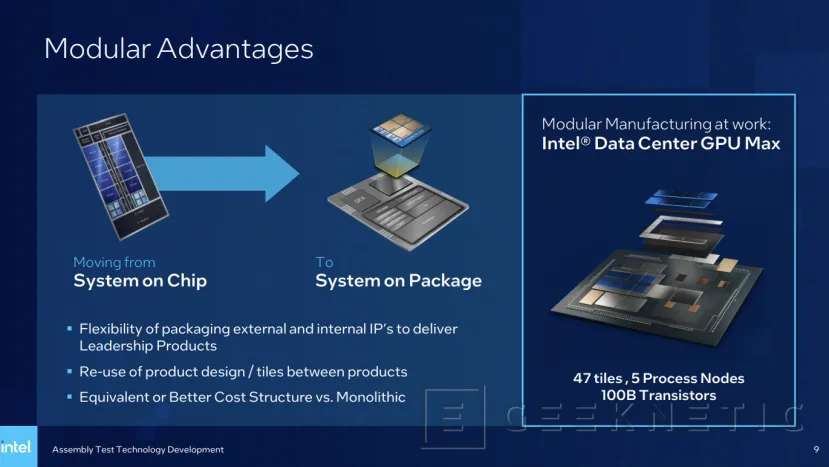
As we said, these technologies have been integrated into different processors throughout history, and currently there has been a shift from SoCs (System on Chip) technology, to what we could call SoP (System on Package), where processors are no longer single chips but multiple chipsets running simultaneously in the same package.
An example of this is the GPU for data centers. Max GPU, better known as Ponte Vecchio, where no more and no less than 47 “tiles” or chiplets have been integrated, with 100,000 million transistors and the combination of 5 different manufacturing processes. It is the most complex chip created by the company and, without a doubt, it marks the way for the future of supercomputing and the application of packaging when creating new, increasingly capable processors.
Creating such a chip in a single manufacturing process would be vastly more expensive and difficult than combining different chips with more basic designs.
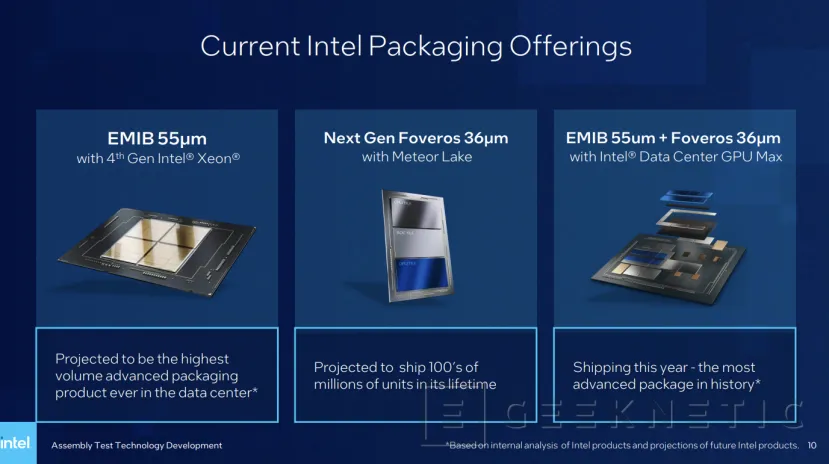
Intel is one of the few companies that has its own manufacturing capability with advanced nodes, alongside TSMC and Samsung. Today, the well-known processor manufacturer offers three packaging technologies. On the one hand we have 2.5D EMIB, used in the fourth generation Intel Xeon Sapphire Rapids processors, EMIB will allow the largest volumes of packaging for data centers to be achieved.
The next generation of Foveros will debut with Meteor Lake, the fourteenth generation of Intel Core processors.
Finally, the combination of 2.5D EMIB and 3D Foveros will give rise to the Intel GPU Max “Ponte Vecchio” GPUs, achieving the most advanced packaging ever with these chips that combine 47 dies with 5 different manufacturing processes at the same time.
Looking ahead, the aforementioned 3D Foveros Direct technology with direct copper connectivity between layers will offer higher performance when interconnecting the dies and, consequently, the final chip.
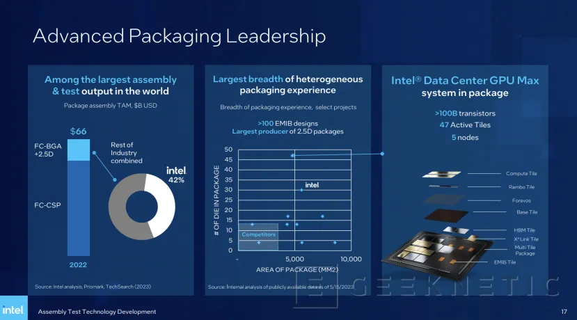
The first Intel customers to make use of Intel’s new advanced packaging technologies will be Amazon’s AWS server division. On the other hand, potential customers also represent the top 10 semiconductor companies without their own manufacturing capacity.
Glass will replace Silicon in the next generation of Intel Packaging
And for the next generation new materials will be introduced, such as interconnection substrate based on a crystal core and optical connections.
This technology will allow greater scalability and achieve compliance with Moore’s Law with higher densities, something that, by then, will be difficult to achieve with silicon.
Current silicon-based packages are beginning to show a slowdown in scaling, and moving to glass will enable further scaling in the future. He glass has a higher dimensional stability, which means that bending or size reduction problems are avoided when creating chips at a few nanometers. Intel’s idea is that the glass replaces the current organic solutions while maintaining compatibility with the designs, allowing to continue using designs already planned with this new technology.
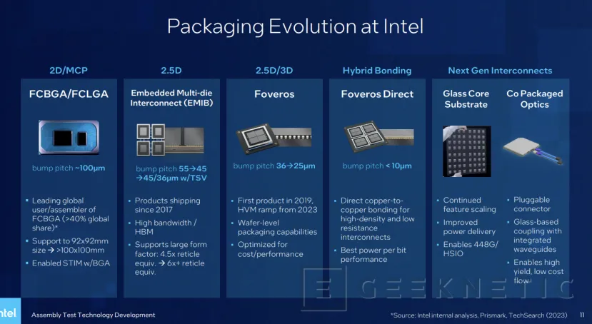
For the user, the use of glass will allow more powerful and efficient chips, with smaller sizes and facilitating manufacturing, which will reduce costs.
Currently, this type of interconnection based on glass substrates cannot yet be integrated because the technology needed to work with this material is very different from that of traditional silicon. But in the future it will be a necessity.
Besides, Intel plans to make its packaging system based on crystal interconnect layers compatible with conventional silicon chips.which will make it possible to create processors and chips for other companies that use traditional designs.
As for the optical connector system, glass will also be used as a material and will allow processors and chips to be connected directly with high-bandwidth cables in rack systems and high-performance servers, for example.
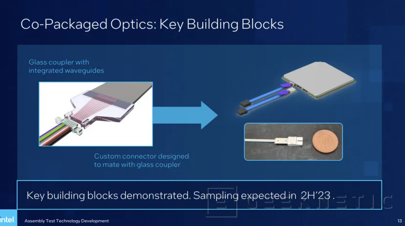
This optical interconnection system will allow chips to be joined by means of its own connector, test modules will begin to be sent throughout the second half of this year.
End of Article. Tell us something in the Comments!


![[Img #74683]](https://thelatestnews.world/wp-content/uploads/2024/12/The-main-mistakes-to-avoid-when-betting-on-electronic-sports-150x150.jpg)


