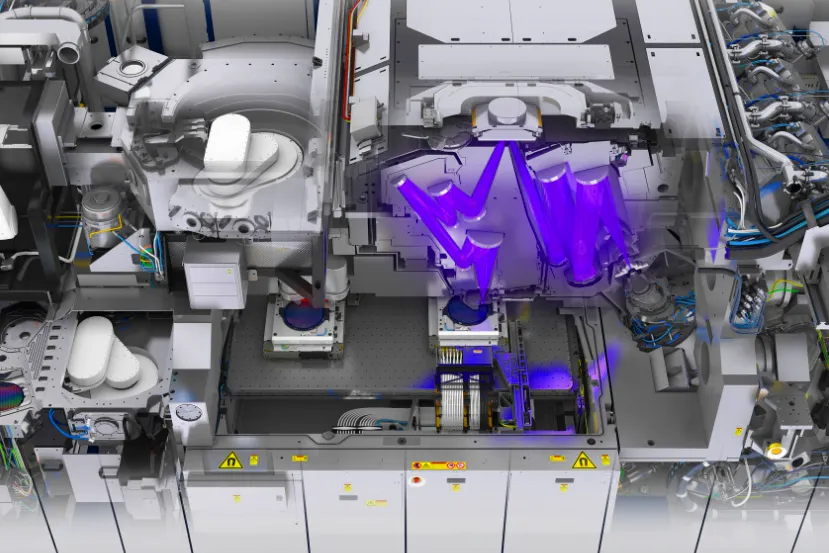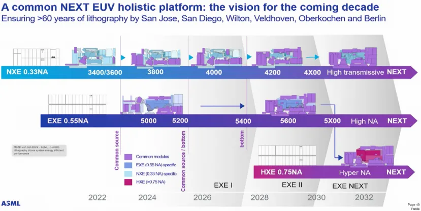
At the beginning of the year, Intel boasted of having received the first ASML lithography machines equipped with High-NA technology. These machines, so called because they use high aperture systems (High Numerical Aperture), are used for the creation of chips with more advanced processes, going from 0.33 NA aperture of the most advanced machinery to date, to 0.55 NA opening.
Although High-NA machines are not yet used for the manufacture of final products (they are expected to arrive with the Intel 18A process in specific parts of the chips), ASML has already sleepless his plans for the next machinery called Hyper-NA EUV (Extreme Ultraviolet Lithography) with a numerical aperture capable of going up to 0.75 NA.

This machinery will allow the creation of even smaller transistors to increase chip density when High-NA machinery begins to encounter limitations in going down to fewer nanometers. This machinery is expected to come into use at the beginning of the next decade of the 2030s.
At the moment, Intel is the only one that uses High-NA machinery, but it is expected that other companies like Samsung will also make the leap. For their part, TSMC seems to be comfortable with the current 0.33 and use “dual pattern” processes to achieve the same as High-NA. However, at some point they will find the limit of this technology and could make the leap to High-NA or directly go to Hyper-NA.
ASML remains the only manufacturer capable of developing this type of EUV machinery for advanced processes.
End of Article. Tell us something in the Comments!

Antonio Delgado
Computer Engineer by training, editor and hardware analyst at Geeknetic since 2011. I love to tear apart everything that passes through my hands, especially the latest hardware that we receive here for reviews. In my free time I tinker with 3D printers, drones and other gadgets. For anything, here you have me.


Add Comment