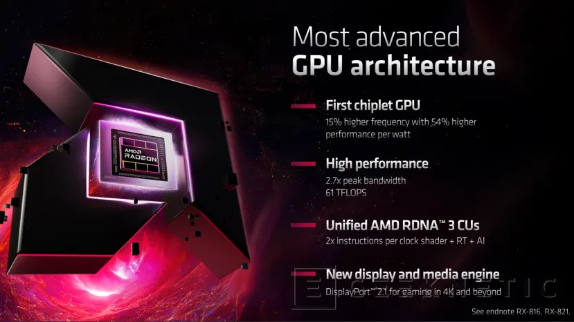
The day finally arrives when AMD launches its next generation dedicated graphics solution, and it does it last, behind Intel and NVIDIA, who have launched the Intel Arc and NVIDIA RTX 40, respectively. Nevertheless, AMD has arrived to present RDNA 3a chiplet-based architecture that has with up to 54% more performance per watt and a catalog of surprises under the arm.
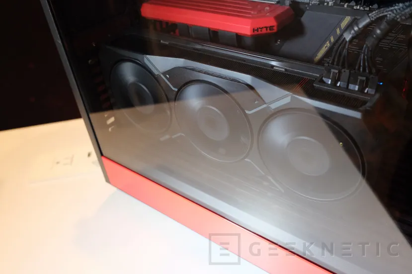
Given this architecture, we find two new top-of-the-range graphics cards, and these are the AMD Radeon RX 7900 XT and Radeon RX 7900 XTXtwo models that arrive as a sample of the most powerful that AMD has to offer us today, but that will be accompanied in the future by less powerful models, with more affordable prices for other enthusiasts.
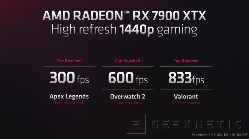
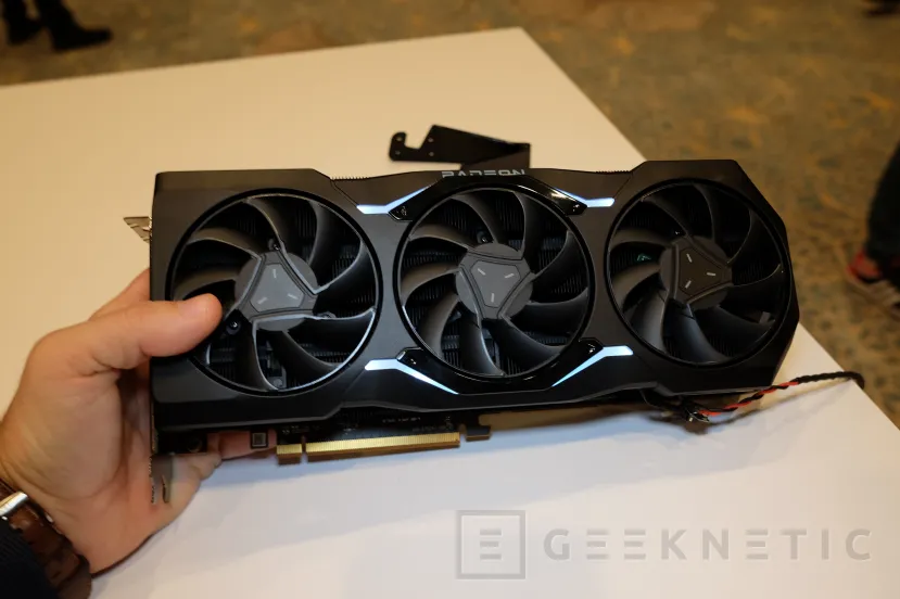
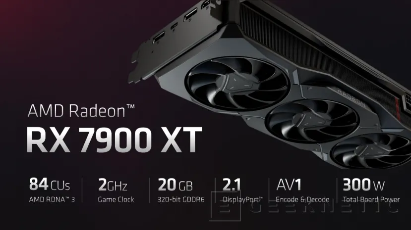
In the case of the AMD Radeon RX 7900 XT, we find a card equipped with 84 CUs RDNA 3 at 2GHz, 20GB of GDDR6 memory connected through a 320-bit wide bus and a consumption of 300W for the complete card, something that rewards us with a much smaller overall card size than Intel alternatives, practically matching the size of the RX 6900 XT.
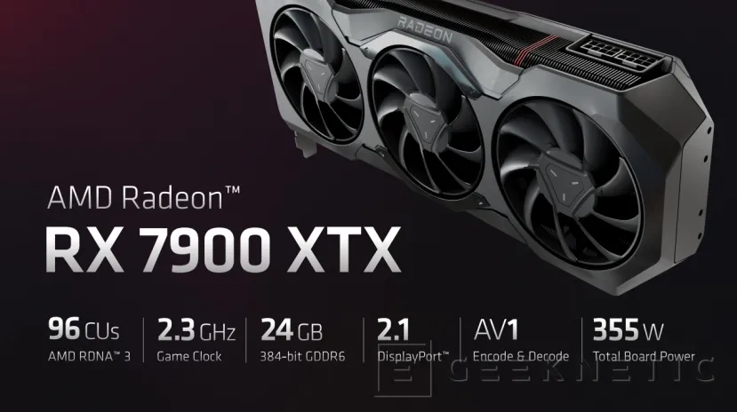
For its part, the AMD Radeon RX 7900 XTX features a total of 96CUs at 2.3GHz and 24GB of GDDR6 memory across a 384-bit wide bus, plus DisplayPort 2.1 support and support for AV1 encoding and decoding on both cards. However, in the case of this model, we find a 355W maximum power and a size similar to that of the RX 6950 XT.
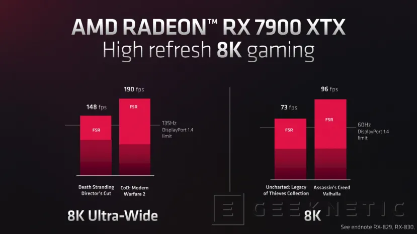
As we see in the performance results of the AMD Radeon RX 7900 XTX, thanks to FSR 3 we will be able to play at 8K Ultrawide resolutions at speeds greater than 135Hz, the upper limit of DisplayPort 1.4, as well as at speeds above 60Hz in standard 8K resolutions, where this limit is also located.
RDNA 3 also comes with a new Media Engine capable of AV1 encoding and decoding, something we’ve already mentioned, but it also has up to 7 times higher performance when transcoding video in 8K resolutions in FFMPEGsomething that requires great performance from the GPU.
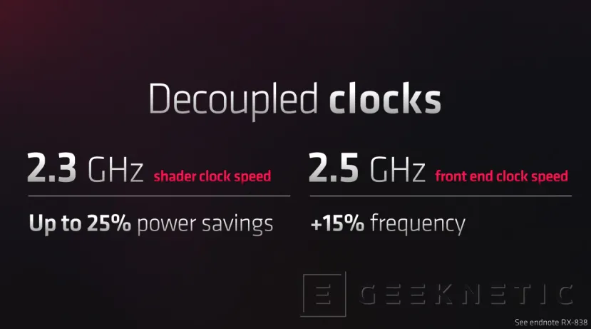
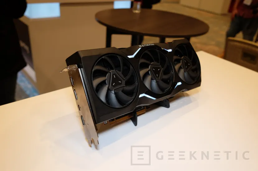
This GPU architecture is based on a chiplet construction, something that involves two different types of chips that we can run at different frequencies from each other. That is why the shaders will work in this case at 2.3GHz, while the front clock speed will be 2.5GHzdelivering increased performance where it matters, while saving up to 25 percent power in the shader department.
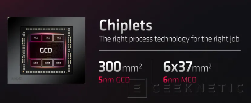
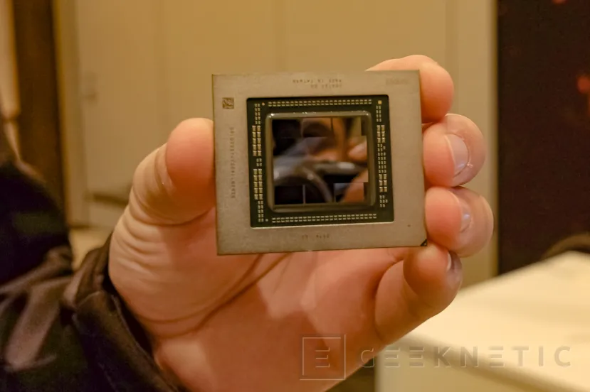
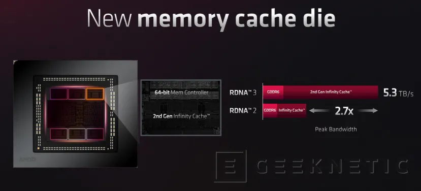
This is also noticeable in the manufacturing processes used, as we find a 300mm square central die manufactured in a 5 nanometer process, which will be in charge of the bulk of the performance, something that its name Graphics Compute Die denotes. However, around it we find six 37 mm square chiplets each manufactured at 6 nanometers, which fulfill the function of Memory Cache Die.
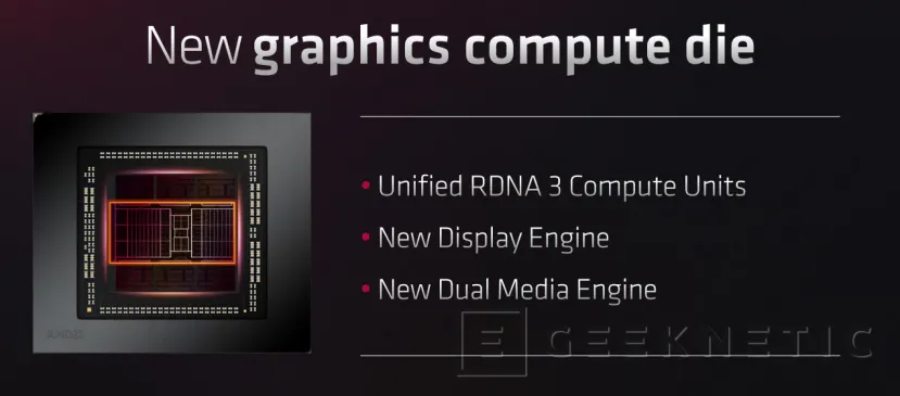
It should be noted that on the RX 7900 XT, one of these chiplets is not electrically functional, but will still be there, possibly to ensure greater stability of the heatsink mounting system, which will improve temperatures by ensuring uniform mounting pressure, something that might not be the case if this chiplet has been physically removed, reasoning why AMD has decided to keep it.
End of Article. Tell us something in the Comments!


